GlobalWafers is a global leader in the manufacture and sale of wafers and related products to the semiconductor industry. Wafers are the foundation upon which virtually all of the world’s integrated circuits are built. Those products, in turn, are the building blocks for the $1 trillion electronics market (cell phones, computers, PDAs, CD/DVD players, satellite and automotive electronics, etc.). GlobalWafers has been a pioneer in the design and development of wafer technologies since 1959, and operates facilities in the U.S., Europe and Asia Pacific.
GlobalWafers can provide both standard and customized silicon wafers to meet your needs.
Analog/Discrete
The tables below are designed to provide you with a quick-reference guide to potential silicon wafer solutions to specific device applications. Common segment drivers and problems are identified and characterized by bulk, surface, or integration issues. Solutions to problems are recommended and a quantitative and qualitative benefit analysis is provided.
B - Bulk; this refers to the ntire lateral and vertical region between the wfer front and back sides. S - Surface; the surface region of a silicon wafer (usually refers to top 10μ) I - Integration; the degree of ease in which the silicon wafer can be integrated into the device manufacturer's line.
Long cycle time and high processing cost due to long thermal treatment steps in the IC fab process that are exclusively designed for denuding.
Starting polished wafer with built-in denuding and nucleation that does not rely on long thermal treatments in the IC fab process.
MDZ
EPI
Furnace cycle time reduction or throughput increase. Reduced thermal budget up to 35%. Saving in furnace capital expenditure or operation cost.
Device Die Yield, Reliability
B
Excessive PN junction leakage current due to OSF, heavy metallic contamination or oxygen precipitates in the sub-surface.
Efficient gettering to effectively getter high levels of metals such as Copper, Nickel, and Iron.
MDZ
Improvement of device reliability.
Device Die Yield, Reliability
S, B
Diffusion of ungettered metals to the active device region, causing leakage or device short.
Robust, consistent gettering independent of initial oxygen level and thermal history. Improves gate oxide integrity (GOI) issue.
MDZ
Yield increase up to 2%.
Device Die Yield
S, B
Furnace slip, dislocations, especially at high temperature steps such as buried layer diffusion and subsequent epi growth.
Increase oxygen level to lock dislocations without allowing precipitates to grow large, improving slip resistance.
Increase slip resistance by nitrogen doping.
Smooth edge.
MDZ
EPI
Annealed
Yield increase up to 1%.
Enhance RF Performance
I
The magnitude of the quality factor degradation of passives at high frequency is larger with the high carrier (low resistivity) density in the substrate, limiting the integration of passives with CMOS or BiCMOS DMOS.
Higher resistivity lowers the parasitic substrate capacitance and eddy current loss in the substrate.
High-Resistivity Polished Wafer
Annealed
Higher Q-factor of inductors and MIM capacitors at RF frequency.
Excess PN junction leakage current due to furnace slip, dislocations.
Optimized oxygen concentration.
Controlled oxygen precipitation.
Smooth edge.
Optimized loading/unloading temperatures and ramping rates of thermal cycles.
MDZ
EPI
Increased device die yields from reduced leakage currents.
Device Yield, Enhance Reliability
B, S, I
Excess PN junction leakage due to OSFs, heavy impurity metallic contamination or oxygen precipitates in the sub-surface.
Diffusion of ungettered heavy impurity metals to the active device region.
Efficient gettering to effectively getter high levels of metals such as Copper, Nickel, and Iron.
Controlled oxygen precipitation with good precipitate-free zone.
MDZ
EPI
Increased device die yields from reduced leakage currents.
Device Yield
B, I
Loss of dies with the breakdown-blocking voltage lower than the rated voltage.
Good uniformity of epi resistivity and thickness.
EPI
Increased BV die yields due to breakdown-voltage above the rated voltage
Device Yield
B, I
Loss of dies with high on-state resistance.
Good uniformity of epi resistivity and thickness.
EPI
Increased Rds (on) yields of MOSFETs.
Increased hFE yield of bipolar.
Conduction power loss, high heat dissipation.
B, I
On-resistance needs to be lowered to decrease power loss.
Limitation to the lowest on-resistance of newer generation power devices.
Low resistivity substrate.
Arsenic doped substrate.
Red phosphorus doped substrate.
Lower power consumption.
Improved power figure of merit without BV tradeoff.
Increased process design flexibility.
Processor/CMOS Logic
The tables below are designed to provide you with a quick-reference guide to potential silicon wafer solutions to specific device applications. Common segment drivers and problems are identified and characterized by bulk, surface, or integration issues. Solutions to problems are recommended and a quantitative and qualitative benefit analysis is provided.
B - Bulk; this refers to the entire lateral and vertical region between the wafer front and back sides. S - Surface; the surface regions of a silicon wafer (usually refers to the top 10μ). I - Integration; the degree of ease in which the silicon wafer can be integrated into the device manufacturer's line.
Maintain dimension scaling to increase performance and functionality.
Integration of ultra-flat wafer processing to improve site flatness and minimize wafer edge roll off.
Epi (P/P+)
Epi (P/P++)
w/ caustic etch & advanced single side polish (200mm)
Improved site flatness enables photolithography process to print smaller critical dimensions.
Excellent nanotopography for critical dimension scaling and CMP uniformity.
High Device Yield for Aggressively Scaled Critical Dimension
S, B
Maintaining high yield with smaller feature size and increased device density.
Epi on P+ or P++ substrate for COP-free and oxygen precipitate-free layer, gettering, and latch up resistance.
COP-free wafer with internal gettering and oxygen precipitate-free zone.
Epi on P- substrate for COP-free and oxygen precipitate-free layer.
Epi (P/P+)
Epi(P/P++)
Ar-Annealed
Optia
High Device Yield.
Device Die Yield, Reliability
S, B
Diffusion of ungettered metals to the active device region, causing leakage or device short.
Robust, consistent gettering independent of the initial oxygen level and thermal history. Improves gate oxide integrity (GOI) issue.
MDZ
Optia
Yield increase up to 2%.
Enhance Performance
S, I
Increase transistor drive current to increase operating frequency.
<100> notch/channel orientation.
<100> notch oriented device layer
10% PMOS drive current enhancement through improved
COP-free wafer with Internal Gettering and Oxygen Precipitate-free zone.
Ar-Annealed
Optia
Epi (P/P+)
Epi (P/P-)
High Device Yield.
Radio Frequency CMOS
S, B, I
Integrate high quality factor passive components and isolate RF/analog components from digital CMOS
High resistivity silicon.
High resistivity silicon on insulator.
Ar-Annealed
~100% increase in inductor Q-factor for 10x increase in resistivity.
Enhance Performance
S, I
Increase transistor drive current to increase operating frequency.
<100> notch/channel orientation.
Ar-Annealed
Optia
Epi (P/P+)
Epi (P/P-)
10% PMOS drive current enhancement through improved channel mobility.
Memory
The tables below are designed to provide you with a quick-reference guide to potential silicon wafer solutions to specific device applications. Common segment drivers and problems are identified and characterized by bulk, surface, or integration issues. Solutions to problems are recommended and a quantitative and qualitative benefit analysis is provided.
B - Bulk; this refers to the entire lateral and vertical region between the wafer front and back sides. S - Surface; the surface region of a silicon wafer (usually refers to top 10μ). I - Integration; the degree of ease in which the silicon wafer can be integrated into the device manufaturer's line.
Minimize impact of COP related yield degradation (leakage, trench to trench shorts (trench technology) and isolation failures).
1) Wafers completely free of COPs.
2) Wafers with COP free surface region.
Perfect Silicon
Ar Annealed
Yield improvement, reliability improvement.
Device Yield
S
Minimize effect of near surface oxygen precipitates (device leakages, trench to trench shorts (trench technology), isolation failures, and non-uniform RIE).
Wafer with no near surface oxygen precipitates (denuded zone structure).
MDZ
Optia
Ar Annealed
Improvement in device reliability.
Device Yield
S
Minimize impact of surface metals (device leakage, isolation failures, and non-uniform RIE).
Tunnel Oxide quality is a critical requirement for flash. Killer defect for leakage failure is point defect such as COP and Metal precipitation on TNOX layer.
COP-free wafer with MDZ. COP-free translates to defect-free material.
Optia
MDZ
Perfect Silicon
MDZ provides robust gettering, which prevents metal contamination.
Optia provides COP-free options as Perfect Silicon.
Enhance Reliability, Device Yield
B, I
Flash device is extremely sensitive to COP defects and metal contamination. Therefore, GOI is a critical concern.
COP-free wafer with MDZ. COP-free translates to defect-free material.
Optia
MDZ
Perfect Silicon
MDZ provides robust gettering, which prevents metal contamination.
Optia provides COP-free options as Perfect Silicon.
Device Yield
B, I
Metal Contamination from backside grinding or dry-polishing.
P/P+ Epi provides a good gettering solution.
Optia
MDZ
P/P+ Epi
1) P+ material has minimum gettering requirement.
2) A polished wafer provides a cost advantage (Optia).
Optia has epi-like GOI and COP-free characteristics.
MDZ provides robust gettering, which prevents metal contamination.
Device Yield
B, I
Yield loss due to gate oxide integrity (GOI) issues.
Rapid thermal process based on technology in which the oxygen precipitation behavior is controlled by manipulation of vacancy rather than oxygen concentration profiles.
Optia
MDZ
Yield improvement up to 10%.
Processing Cost
B, I
Increased processing costs due to long thermal treatments.
Optia wafers do not rely on thermal treatments in the IC fab process.
Optia
MDZ
Reduce thermal budget up to 40%.
MDZ reduces cost of ownership (COO) due to lower thermal budget in the IC fab.
Enhance Reliability
B, S, I
Device loss due to metal contamination.
Optia will effectively getter high levels of metals such as Copper, Nickel, and Iron.
Optia
MDZ
Improvement in device reliability.
Device Yield
B, S, I
Crystal defect related yield and reliability degradation.
Elimination of harmful crystal defects in the surface and bulk.
Optia
MDZ
Yield improvement, reliability improvement.
Perfect Silicon crystal results in a defect-free wafer.
Device Yield
B, I
Yield loss due to uncontrolled precipitation of oxygen.
Rapid thermal process based technology in which the oxygen precipitation behavior is controlled by manipulation of vacancy rather than ocygen concentration profiles.
Optia
MDZ
MDZ provides required BMD densities that demonstrate uniform stacking faults and precipitate distribution.
Device Yield
S, I
Nanotopography and flatness issues.
Need uniform flatness center-to-edge to print very small feature sizes.
Optia
Extend usable edge area, which increasesthe number of usable die per wafer.
Enhance Reliability, Device Yield
B, I
Stored charge leakage due to tunnel oxide quality.
COP-free wafer with MDZ and OOBG.
Optia
MDZ
Yield improvement, reliability improvement.
Polished
Standard Wafer
Our principal product is the prime polished wafer: a highly refined, ultrapure wafer of crystalline silicon with ultraflat and ultraclean surfaces, that is custom built to meet customer specifications. Sophisticated chemical-mechanical polishing (CMP) processes remove surface defects and produce extremely flat, mirror-like surfaces. The CMP process was pioneered by GlobalWafers in 1962 and is still the industry standard today. Prime Polished silicon wafers are used in broad range of advanced integrated circuit applications by our customers.
Improve Device Performance, Reliability, and Cost of Ownership
Advanta™ wafers have low COPs (crystal-orginated pits) and high GOI (gate oxide integrity) performance. Advanta's annular region outside of a central vacancy core is free of any agglomerated defects. Advanta wafers can be enhanced using GlobalWafers' Magic Denuded Zone® (MDZ®) thermal treatment. MDZ® produces robust internal gettering protection early in the IC fabrication process.
Reduced COPs lead to higher reliability related to crystal defects
Comparable performance with annealed wafers at much better cost
Deep precipitate-free zone through MDZ® maintained throughout customer processing leads to improved device yield and reliability potential
Built-in IG template through MDZ® eliminates need for customer oxygen out-diffusion and nucleation and reduces customer cycle time
Improve Device Performance, Reliability, and Cost of Ownership
The OPTIA™ wafer is a high performance silicon substrate for the VLSI and ULSI IC device generations. These devices are built today with increasingly denser and more complex architectures. Consequently, increasingly tighter specifications are required for silicon substrates. Crystal-related defects in the wafers have been correlated with decreased GOI (gate oxide integrity) performance. OPTIA™ wafers have zero crystaloriginated pits (COPs) and epi-like GOI, therefore, they provide an ideal solution for next generation IC devices. OPTIA™ wafers are free of agglomerated defects across the wafer and throughout the whole wafer thickness. OPTIA™ wafers are enhanced using GlobalWafers' patented Magic Denuded Zone® (MDZ®) thermal treatment. MDZ® produces a deep precipitate free zone and provides robust internal gettering protection early in the IC fabrication process.
No harmful crystal defects in the surface and bulk leads to no crystal defect-related yield and reliability degradation
Better quality, performance and cost of ownership than annealed wafers
Deep precipitate-free zone through MDZ® maintained throughout customer processing leads to improved device yield and reliability potential
Built-in IG template through MDZ® eliminates need for customer oxygen out-diffusion and nucleation and reduces customer cycle time
The Argon Annealed wafer is an advanced prime wafer which provides a defect-free surface region for high device yield and internal gettering for resistance to contamination. The combination of a nitrogen doped crystal and a high temperature furnace anneal in an argon ambient creates a defect free near-surface region, an oxygen denuded zone and a bulk oxygen precipitate density with internal gettering ability.
Argon annealed wafers are used in advanced CMOS technology processes and offer a yield advantage for polished wafers.
Argon annealed wafer cross section
COP-free and oxygen denuded zones for high device yield potential and oxygen precipitates in bulk for immediate gettering in device process.
Surface COP annihilation during high temperature argon annealing
Step 1: Oxygen above solubility limit. Oxide layer inside “bulk” COPs increases in thickness. COPs do not dissolve.
Step 2: Oxygen below solubility limit. Oxide layer inside “surface” COPs decreases in thickness. Once oxide layer no longer present, COPs first shrink and then dissolve through point defect interactions.
Physical model of COP annihilation: M.Hourai, et al., Defect in Silicon III, The Electrochemical Society PV 99-1, p. 372, 1999
Impact of COPs on Device Yield
COPs are known to increase gate oxide defect density for oxide thickness ≥ 100 Å. Recent reports such as Itsumi’s suggest that COPs may not be as harmful to GOI for oxides < 100 Å.
Si wafer suppliers have generally confirmed Itsumi’s observations although recent GlobalWafers development programs appear to show a small but non-zero influence of COPs on defect density.
COPs are reported to decrease CMOS device yields by increasing field oxide leakage and junction leakage.
COPs interfere with the fabrication of high density, sub-100 nm gate length transistors when these fall into the surface pit associated with a COP.
Benefits of argon annealed wafers
COP-free surface zone ≥ 10μm
High GOI yield
Low surface light scattering counts (LLS’s)
High device yield potential
Out of Box Gettering (OOBG)
Annealing creates well defined denuded zone of ≥ 20μm
BMDs present in an annealed wafer ensure immediate gettering for low thermal budget processes
BMD density ≥ 5x10⁸ defects/cm3
Meets all advanced wafer parametric requirements for global and local flatness, warp, surface roughness, and metals
We supply test and monitor wafers to our customers for use in testing and controlling semiconductor fabrication lines and processes. Although monitor wafers are substantially the same as prime polished wafers with respect to cleanliness, and in some cases flatness, other specifications are generally less rigorous. This allows a more cost-effective solution for non-critical wafer applications.
The trend to produce smaller and smaller device features began in 1958 with the invention of the first integrated circuit in order to incorporate more complex functionality. Smaller device features also improve performance and reduce power consumption and heat production in the circuit. A critical aspect in the construction of any integrated circuit is the electrical isolation of the circuit elements from each other. Without sufficient isolation, the elements could communicate electrically with each other in unintended ways, ruining device performance. Smaller device features reduce the distance between circuit elements, exacerbating isolation problems, as well as increasing sensitivity of the devices to minute surface imperfections in the wafer.
Our epitaxial wafers meet the technological demands of our customers that manufacture advanced semiconductor devices. Epitaxial wafers consist of a thin, single crystal silicon layer grown on the polished surface of a silicon wafer substrate. This "epi" layer is designed to have different compositional and electrical properties from the underlying wafer, tailored to the specific demands of the device. This compositional change, among other things, can be used to improve isolation between circuit elements fabricated on the epi wafer. The epi layer is also substantially free of surface imperfections that can cause device failure. Epitaxial wafers provide for increased reliability of the finished semiconductor device, greater efficiencies during the semiconductor manufacturing process, and ultimately more complex integrated circuit devices.
Traditionally, power discrete devices and power IC's are built on an epitaxial wafer because it provides the device fab with a great controllability of series resistance (or conductivity) in the base of diodes, rectifiers, thyristors, or bipolar junction transistors (BJT), or in the drift zone of MOSFETs and IGBTs. Typically, thin base or drift is preferred, which is achievable and cost-effective using epi wafers. Additionally, an epi wafer's inherently uniform resistivity distribution, both from wafer to wafer and within the wafer, provides additional benefit. Lower resistivity of the epi layer is the preferred solution for lower Rds(on), but it may cause breakdown voltage to be below the acceptable level. As a result, the resistivity and thickness specifications for power discrete epi wafers are very tight. Rds(on) is the series resistance of the device during its "on" state that is a very critical parameter and affects the device's power consumption. GlobalWafers provides epi wafers specifically for power MOSFET, bipolar and other discrete applications. Combinations of N-type and P-type epi layers and heavily doped substrates are offered for these applications.
Epi Reactor
Diameter
Type
Epi Thickness Target, UM
Epi Resistivity Target, Ohm-cm
Uniformity, +/-%
Grade
Epi Resistivity
Epi Thickness
Batch
150mm 200mm
P/P++ N/N+ N/N++ N/N+/N++ N/P/P+ P/N/N+
3-70
0.2-30
Standard
8-10
5-8
Enhanced
6
4
Single Wafer
150mm 200mm
P/P++ N/N++ N/N+/N++
3-30
0.1-30
Standard
5
5
Enhanced
3
2
Certain power discrete devices such as IGBT and special BJT products are built in a double-layer epi and, in a special case, a triple-layer epi to simplify device process design or reduce fabrication cost. For example, IGBT epi wafer has two layers of epi deposited onto heavily doped substrate of the opposite type (e.g., N/N+/P++.) A special BJT epi wafer has double layers of epi deposited onto heavily doped substrate of the same type (e.g., N/N+/N++.) Another special BJT epi wafer has two layers of epi of the opposite type (e.g., N/P/P++). Multiple layer epi wafers are mostly used for high voltage/power devices and tend to be thick. However, the resistivity uniformity of multiple-layer power discrete epi wafers is comparable to that of single layer epi with the same thickness. )
Sub Dopant
Resistivity Target, Ohm-cm
Diameter
Boron
<0.001-0.02
150mm, 200mm, 300mm
Arsenic
0.0017-0.007
150mm, 200mm
Phosphorus
<0.001-0.003
150mm, 200mm
Antimony
0.005-0.03
150mm, 200mm, 300mm
Red phosphorus doped substrate for epi: The resistance of epi substrate is also an important component of the series resistance of power discrete devices and its contribution to the final device Rds(on) becomes increasingly significant in low voltage (<= 30V) power devices, such as cell phones and other hand-held electronics where low power consumption is most critical to long battery life. The beneficial effect of low resistivity substrate is particularly important, as it does not limit breakdown voltage. Achieving low Rds(on) by using very low resistivity substrate can eliminate the need to develop the next technology platform, and thus reduce cost and time to market. For this matter, n-type epi deposited onto n-type substrate with very low resistivity (e.g., < 0.0015 ohm-cm) suits the need, which is achievable through the recent development of elemental red phosphorus doped crystal growth technology.
A variety of epi products having features uncommon in standard CMOS or power discrete epi products are demanded for special purpose. These are categorized as "custom epi" and are made to order either in-house or through qualified outsourcing partners that are specialized in silicon epitaxial growth.
Custom EPI Product Examples
Product
Diameter
Features
Intrinsic or pseudo-intrinsic layer epi
150mm
200mm
N(i)/P+ Intrinsic(or psuedo-intrinsic) resistivity > 200 ohm-cm with no upper limit
N(i)/N++ Intrinsic(or psuedo-intrinsic) resistivity >> 50 ohm-cm with no upper limit
P(i)/P+ Intrinsic(or psuedo-intrinsic) resistivity >> 30 ohm-cm with no upper limit
Graded doping epi
150mm
200mm
Tailored doping profile
Ultra thick single layer epi
150mm
200mm
>70 um
Ultra thick multiple layer epi
150mm
200mm
>70 um total cumulative
Heavily doped layer epi
150mm
200mm
300mm
P+(<0.02 ohm-cm)/P+
P+/N++
N+/P++
As-doped layer epi
150mm
N/P++
As doped to <0.05 ohm-cm
Epi on ultra high resistivity substrate
150mm
200mm
P/UHR Cz (Substrate > 1000 ohm-cm)
Perfect Silicon
Perfect Silicon™ brand wafers utilize GlobalWafers' proprietary defect-free crystal growth process designed to completely suppress the formation of low-density, grown-in defects. The main principle behind the CZ single-crystal growing process lies in the rapid transport of growth-incorporated excess intrinsic point defects to harmless sinks before they have a chance to react to form defects. This method of growing CZ single-crystal controls the point defect level such that there is no excess concentration above thermodynamic equilibrium, thereby preventing clustering as the crystal cools. Such material is said to be grown under unique, dynamic quasi-equilibrium conditions. The as-grown crystal is completely defect-free, and therefore, requires no post-growth engineering, such as annealing or epitaxy.
This leads to a very homogenous silicon wafer with zero defects. Perfect Silicon brand wafers are the most advanced silicon materials available in the world today:
free of agglomerated defects across and throughout the whole wafer thickness.
100% free of COP, D-defect, I-defect, etc.
no need for post-growth engineering such as annealing or epitaxy.
robust internal gettering and PFZ provided by patented MDZ® treatment if required by customer.
Magic Denuded Zone
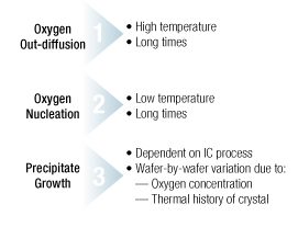
Magic Denuded Zone® (MDZ®) is a patented, rapid method of achieving reproducible and reliable internal gettering in silicon wafers. It is a Rapid Thermal Process (RTP) based technique in which the oxygen precipitation behavior is controlled by the manipulation of vacancy rather than oxygen concentration profiles. GlobalWafers has engineered the RTP process to create a vacancy concentration depth profile that effectively preprograms the precipitate-free zone depth and precipitate density of the wafer to ideal targets. MDZ® produces a silicon wafer with ideal oxygen precipitation behavior, and reproducible and reliable IG which is nearly independent of the initial oxygen concentration, the thermal history effects from crystal growth, and the IC fab process application.
Magic Denuded Zone®, MDZ®, and the MDZ® logo are registered trademarks of GlobalWafers Inc. All rights reserved.
The MDZ® process is protected by the following patents:5,994,761; 6,180,220; 6,204,152; 6,306,733; 6,586,068; 6,849,119; 6,336,968; 6,432,197; 6,709,511; 6,191,010; 6,579,779; 6,713,370.
The control of oxygen precipitation behavior in all silicon wafer products is a crucially important component of the silicon wafer business because it is important to the successful manufacture of integrated circuits.
There is a degree of unpredictability in the performance of wafers in regard to the behavior of oxygen. Uncontrolled behavior is completely unacceptable. Control of oxygen concentration with the intent of controlling oxygen behavior is not sufficient to deliver optimum performance.
Device manufacturers are concerned with two things related to the behavior of oxygen in the wafers they use to manufacture their devices with:
First and foremost, they are concerned that no oxygen-related defect (precipitate) be the root cause of a measurable yield loss in their finished good.
Assuming the first, necessary requirement is met, they are generally interested in utilizing the internal gettering (IG) potential of bulk oxygen precipitates as a yield maintenance tool.
In other words, not only should the silicon wafer itself not be a yield-limiting factor, but it should be a yield-enhancing factor for our customer.
Over the years, the silicon industry has collected a great deal of costly, excess baggage along the road to satisfying these two conditions.
GlobalWafers' patented MDZ® process and silicon wafer is the ideal solution for the problem of controlling oxygen precipitation in all IC processes. MDZ® wafers are programmed for optimum, robust, and uniform performance. MDZ® greatly simplifies the use of silicon wafers while at the same time bringing a new, and until now, unheard of precision to their performance.
GlobalWafers' patented MDZ® process and silicon wafer is the ideal solution for the problem of controlling oxygen precipitation in all IC processes. MDZ® wafers programmed for optimum, robust and uniform performance. MDZ® greatly simplifies the use of silicon wafers while at the same time bringing a new, and until now, unheard of precision to their performance.
The source of all unpredictability – and hence complication – in standard silicon wafers can be traced to the difficulty in controlling all the coupled oxygen reactions which take place during crystal growth and wafer processing. MDZ sweeps this all aside by wrestling away the control of these reactions and giving it to a new, much easier to control component -– the vacancy.
Reaction-controlling vacancies are installed into silicon wafers by a rapid and positive RTP process which replaces the standard thermal donor anneal step. The installed profile of vacancy concentration effectively and robustly programs the wafer to behave in a certain predetermined way. The MDZ process installs a profile that insures optimum performance for all applications.
By sweeping aside all the oxygen-related complications which have stood for many years as a important barrier to the rational use of silicon wafers in IC processes, the MDZ process removes a huge number of oxygen related complications. The MDZ wafer is simplicity itself. It does not require tight oxygen concentration control to give high performance results; it does not require specific tailoring or tuning of silicon wafer to meet the needs of specific processes; it does not require additional costly heat treatments to insure denuded zones. The details of the crystal growth process is no longer important to oxygen behavior. MDZ simplifies the use of silicon to the degree that one specification -– MDZ -– covers all IC applications.
An MDZ wafer is one simple answer to what used to be a million questions. And it is the best answer.
Why do vacancies enhance the precipitation of oxygen in silicon?
The simple answer is that oxygen precipitates need room to grow inside a silicon crystal. They are larger than the silicon lattice and thus introduce strain as they grow. This strain is the main limiting factor to the nucleation of oxygen precipitates in silicon. Vacancies are effectively represent open space in the lattice and offer a means to relieve this strain.
A more detailed answer
The relief of strain by vacancies is clearly the basic reason underlying the MDZ effect. But the details are more complicated. A more subtle explanation of the strain relief of the ‘magic’ effect of vacancies (oxygen-independent production of precipitates!) is that oxygen clustering, during the nucleation anneal, proceeds by the agglomeration of the vacancy-oxygen species (O2V). The nucleation rate is controlled by the species concentration Cv, and thus independent of the oxygen content. The nucleation rate is a rapidly increasing function of the species concentration Cv. Below some critical concentration Cv*, the nucleation rate becomes negligible.
In the range of low Cv, the agglomerating species are oxygen atoms, and the nucleation rate is then controlled by the oxygen content C. The produced oxygen clusters are strongly strained (unlike the clusters of O2V species). The free energy gain per an atom is m-w, where m=kTlog(C/COi*) is the oxygen chemical potential (COi* is the oxygen solubility) and w is the strain energy. The difference m-w is positive at the nucleation temperature (such as 650oC) but becomes negative at higher T (at 1000oC), since m is then considerably reduced. Thus the nucleated clusters will all dissolve during the precipitation anneal, regardless of their size. The only way for the clusters to survive is to relieve the strain by emission of self-interstitials. The emission rate becomes fast only if the clusters are larger than some characteristic size. This is considered to be the main reason for a long incubation. During the nucleation stage, the clusters need to grow to a size large enough for subsequent efficient emission of self-interstitials during the precipitation anneal. In the case of clusters of the vacancy-oxygen species O2V, there is no problem of strain: the space for a cluster is ‘carried’ by the agglomerating species themselves. Hence there is a negligible incubation time for this vacancy-assisted nucleation.
Is MDZ® really independent of oxygen concentration?
Vacancies really do control the show in the MDZ business. Oxygen is important only as a "construction material". In CZ silicon there is always enough of it around. It never limits the process. MDZ really is independent of oxygen concentration.
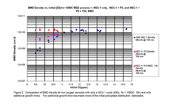
Yet, at low oxygen concentrations (below about 10 pmma) some experiments may seem to show that the MDZ effect rolls off and that there is an oxygen concentration dependence. But this is not true. Simple treatments such as the NEC1 treatment (4 hours at 800°C followed by 16 hours at 1000°C) simply do not tell the true story at low oxygen concentrations. The reason for this experimental error is that at very low oxygen concentrations, the growth treatment (the 1000°C part) necessary to make the precipitates visible is not completely effective. To see the true picture (MDZ is completely independent of oxygen concentration) you have to increase the driving force for precipitate growth (go to lower temperatures) for longer times.
Just because a precipitate is not visible after a precipitation test does not mean it is not an effective gettering site (or for that matter a danger if located near the wafer surface). Quite the contrary.
Oxygen Independence of MDZ
Even at very low oxygen concentrations but beware detection limits
Why is precipitation suppressed in the surface layer of an MDZ® wafer?
The surface region of an MDZ wafer has the same character as a Tabula Rasa wafer. A Tabula Rasa wafer is a wafer in which all the oxygen clusters "grown-in" by the crystal growth process have been dissolved by a brief high temperature wafer treatment. In the case of the MDZ wafer this comes for free during the first phase of the process. It happens on the way up to the process temperature - during the heating-up phase of the process.
A Tabula Rasa wafer not only eliminates the possibility of oxygen precipitates originating at crystal growth but also – in all but extreme and highly unlikely situations – effectively suppresses the future nucleation of oxygen precipitates in process.
In doing so it relies on the phenomenon of "incubation". A long time (typically more than many hours) at low temperatures is required to produce oxygen clusters large enough to grow at a higher temperature.
A very important fact to keep in mind is that the time required to do so is not cumulative. Any high temperature treatment following a potentially nucleating low temperature treatment acts itself a Tabula Rasa treatment - erasing all that came before. The incubation process must then start again from zero during the next low temperature phase.
A more detailed answer:
The MDZ wafer delivers a "real" denuded zone in IC processes in the sense that there are really no precipitates in the near surface region – not just precipitates that you cannot see by common analysis techniques.
How does it do this and how does it ensure that no precipitates form in the near surface region without oxygen out-diffusion?
The major source of oxygen precipitates in the near surface region of a silicon wafer is the existence of small oxygen clusters which form during the growth of CZ crystal. They form in a complex manner as the crystal cools. The usual critical temperature range in which they form is between about 400 and 800°C. Their density distribution is a complicated function of the crystal’s (or rather crystal segment’s) oxygen content, it’s carbon content, the cooling rate through this temperature range, and even – due to more subtle effects – the cooling rate in other, higher temperture – ranges too. The complex interaction of all these effects (together with their interaction with the specific details of the application to which they are submitted) is the main reason for the need of most of the complicated wafer tailoring and specification baggage which has arisen over the last 20 years of applying silicon to advanced IC applications.
When the crystal is cut into wafers these clusters are uniformly distribution throughout the thickness of the wafer. These clusters grow into precipitates during wafer processing. If proper care is not taken, they may form in the near surface region of the wafer resulting in device failure.
Tabula Rasa:
In modern silicon, carbon levels have been reduced to the point where it no longer has an effect as a catalyist to oxygen clustering. Largely as a result of this, oxygen cluster sizes formed during growth are generally restricted. This happy event paved the way for the "Tabula Rasa" process. In today’s low carbon silicon, grown in oxygen clusters may be completely dissolved at the wafer level by short heat treatments at temperatures greater than about 950°C. Such a treatment dissolves the clusters and sends the oxygen contained in them back into solution. It is called "Tabula Rasa" (lat: blank slate) since it effectively erases the "thermal history" or that the crystal has undergone during crystal growth. It’s memory is wiped clean.
Such a wafer produces no oxygen precipitates in standard precipitation test anneals such as the "NEC1 test" (4 hours at 800°C followed by 16 hours at 1000°C). Without a Tabula Rasa anneal the density of oxygen precipitates produced by such a treatment could easily vary over about 5 orders of magnitude – even within the same crystal, and even if the oxygen content were well controlled.
This has long been recognized as a problem. It is, in fact, the main reason why many wafer road maps show the need for oxygen content to drop to very low values in the future. The hope is that a very low oxygen contents the oxygen cluster density produced during crystal growth will be small.
But this is an expensive and really rather silly solution to the problem. Tabula Rasa easily ensures that, regardless of oxygen content, the grown-in cluster density will be zero.
OK, so you’ve eliminated grown-in oxygen clusters from the wafer, how can we be sure that they do not form again?
In the vast majority of real practical cases they will not form again. The Tabula Rasa wafer really does ensure effective suppression of the formation of oxygen precipitates in process. The reason is does this is due to a phenomenon well know to materials science, namely the "incubation effect" in time-dependent nucleation.
During heat treatments, distributions in size of clusters form by adding one atom at a time. In general, these distributions are broad at low temperature (can reach large sizes) and narrow at high temperature (are restricted to small sizes). However, the build up of the distribution over time is strongly dependent on the mobility of the solute atoms at the temperature of interest. At high temperature things move faster than at low temperatures. At high temperatures, the narrow (steady state) distributions are reached quickly, while at low temperatures, the potentially wider size distributions take much longer to form.
It is the speed of reaching high temperature narrow size distributions which ensures rapid Tabula Rasa action: the broad distribution of oxygen clusters formed during crystal growth are rapidly (in a matter of seconds) relaxed to the narrow high temperature distributions. Oxygen precipitates cannot be produced from narrow high temperature size distributions.
But it is possible to produce sufficiently wide distributions of oxygen cluster sizes at low temperatures such that when the wafer is heated to high temperatures the largest of them grows. But this takes a long time. And in fact, the time it takes at low temperature to produce clusters of size large enough to grow at high temperatures is what we call the "incubation time".
This whole process is furthermore limited by the fact that it is only at temperatures below about 750°C that clusters large enough to grow upon subsequent treatment can even possibly form.
As long as the time spent at these temperatures prior to a high temperature treatment is less than the incubation time, the ALL of the clusters produced at low temperatures will relax to the narrow, and harmless, high temperature distribution.
The times required to exceed this are, in general, very long: greater than about 4 hours at 650°C (an "ideal" nucleation temperature) are required for this to happen.
This time is strongly oxygen concentration dependent. Should such long times exist in a given application, then an oxygen concentration sufficiently low to ensure the effective suppression of oxygen precipitation can always be found.
Tabula Rasa wafers have been in widespread and successful use for many years now in a wide variety of applications.
MDZ and Tabula Rasa
A Tabula Rasa wafer is a wafer in which the precipitation of oxygen is everywhere suppressed. Such a wafer meets our goal of not getting in the way of high yields. But it does not add anything to the enhancement of yield. To do this the wafer must contain bulk precipitate sites for effective gettering.
MDZ combines the benefits of Tabula Rasa with precipitation enhancement in the bulk. The Tabula Rasa effect comes for free in the MDZ wafer. As the wafer is heated on its way up to the high process temperatures (and before a vacancy concentration profile is installed) the grown-in clusters dissolve by the Tabula Rasa effect.
After the installation of the vacancy profile, the near surface region contains a low concentration of vacancies. As such it acts as a "normal" wafer. In fact, it acts as a normal Tabula Rasa wafer.
Oxygen precipitation there is suppressed and stays suppressed.
Tabula Rasa material is dead and stays dead.
What bulk precipitate densities are needed to ensure effective gettering?
The major source of the unpredictability of oxygen precipitation in standard silicon wafers is the existence of small oxygen clusters which form during the growth of CZ crystal. They form in a complex manner as the crystal cools. The usual critical temperature range in which they form is between about 400 and 800°C. Their density distribution is a complicated function of the crystal’s (or rather crystal segment’s) oxygen content, it’s carbon content, the cooling rate through this temperature range, and even – due to more subtle effects – the cooling rate in other, higher temperture – ranges too. The complex interaction of all these effects (together with their interaction with the specific details of the application to which they are submitted) is the main reason for the need of most of the complicated wafer tailoring and specification baggage which has arisen over the last 20 years of applying silicon to advanced IC applications
In addition to this there are other effects which further couples the details of the crystal process to the resulting oxygen precipitation behavior. One often important complication relates to the concentrations of residual vacancies grown in to crystal as a result of a completely different phenomenon – that of the formation of voids in silicon crystals. Such an effect is responsible for the commonly observed increase in oxygen precipitation in crystal tail end sections.
In short, the details of the crystal growth process are hugely coupled to the oxygen precipitation performance of "normal" wafers. The constraints this adds to the silicon business is unacceptable in the modern world.
Under what conditions could the vacancy profile of an MDZ wafer be erased before it has time to nucleate the desired bulk oxygen precipitates?
During the installation of the MDZ vacancy profile, the final stage is reached during cooling when the temperature of the wafer drops below 900°C. At this point all the hitherto mobile vacancies are frozen in place through a binding process. The immobile complex O2V is formed. By 900°C all the vacancies in the wafer are bound up in this state. The wafer vacancy profile is fixed in place.
A second "fixing" of our latent precipitate image occurs at temperatures lower than about 800°C. In this range the bound up vacancies are consumed into the oxygen clusters which subsequently grow upon further treatment.
Should a virgin MDZ wafer be heated rapidly (in an RTP furnace) to temperatures greater than 900°C and go through the very rapid low temperature nucleation phase to quickly, then the frozen in vacancies will become free again and will diffuse to the wafer surfaces, relaxing the profile and erasing the MDZ effect.
This erasure effect is strictly limited to the first heat treatment the wafer sees. Following the stabilization phase, the profile can no longer be affected by high temperature treatments.
How can it be that the behavior of MDZ wafers are not dependent on the details of the application to which they are submitted?
The catalysis effect of the vacancies on oxygen clustering is very, very fast. The vacancy profile installed in the wafer is transformed into oxygen precipitate clusters as the wafers are being heated up during the first heat treatment they receive. In the process of transforming into clusters, the vacancies themselves are consumed. Their life and job is over at this point. The clusters that form during this stage merely grow with further processing. Nothing in all but the most extreme (and unlikely) process environment will alter their distribution.
Oxygen & How MDZ is Made
An MDZ wafer relies on the installation of a vacancy concentration profile in a wafer. Where the vacancy concentration is large, a very rapid catalysis of the oxygen precipitation process takes place. Where the vacancy concentration is low, oxygen precipitation is suppressed. A simple inverted U-shaped profile front to back (with the concentration high in the center, low at the surfaces) results in a layered oxygen precipitate structure which is ideally suited for advanced IC manufacture.
A straightforward and reliable process gets the job done in seconds.
When a wafer is heated to high temperatures increasing numbers of silicon atoms leave their lattice sites in the crystal. The numbers that do so are governed by the laws of thermodynamics. When a silicon atom leaves its lattice site it becomes an "interstitial" atom. It leaves behind a "vacancy". Interstitials and vacancies are created in pairs (and thus in equal numbers) in this way -- naturally and predictably simply by heating silicon to a given temperature. Call this "step 1."
In silicon, it turns out, the vacancy is slightly more energetically preferred than the interstitial. Thus in equilibrium there should be more vacancies than interstitials. This is rapidly corrected. Interstitials diffusion phenomenally fast in silicon and the excess interstitials diffuse out to the surfaces of the wafer. After only one or two seconds at temperatures around 1200°C, the wafer has established true temperature dependent equilibrium concentrations of both its vacancies and interstitials. Thus at this stage there is a slight imbalance in the wafer with more vacancies than interstitials. This is critical to the working of the process. Call this stage "step 2". The higher the temperature, the higher the concentration of vacancies. Their concentration is dependent only on temperature. Simple.
As it turns out, the problem is keeping them in the wafer as it cools from the process temperature. As a wafer cools from high temperatures, it tries to keep up with its ever-changing equilibrium state. At lower temperatures, equilibrium requires lower concentrations of vacancies and interstitials. There are two ways the wafer can try to keep up with equilibrium (that is: get rid of the excess vacancies and interstitials) as the wafer cools.
One way is for the intersititial atoms to fall back into the vacancy sites (or "recombine"). But recall that in step one, we created an imbalance in the concentrations of the vacancies and interstitials. There are simply not enough interstitials around anymore to fill all the vacancies. Thus As the wafer cools, the vacancy concentration is reduced in accordance with the dictates of equilibrium by interstitials falling back into vacancies – but only up to the point at which we run out of interstitials. This occurs rapidly - after about 50 degrees of cooling, typically. Cooling further the remaining vacancies become "supersaturated". These are the vacancies that will later be doing our job of enhancing the precipitation of oxygen.
But this is not the end of the story. There is another avenue for some of the vacancies to take in trying to maintain equilibrium. Those vacancies which are sufficiently close to the surface can diffuse there and recombine. The surface of a wafer may be considered to be an infinite sink for excess vacancies (and interstitials). But diffusion from the interior of the wafer to the surface takes time and is limited by how fast the vacancies can be transported there. Thus, depending on the cooling rate, various depths of the silicon beneath the surface are "cleaned out" of vacancies by transport to the surfaces.
If the cooling rate is too slow – such as is always the case with furnace heat treatments, then effectively all of the excess vacancies are cleaned out of the wafer through the surfaces. This is in fact the usual case for a furnace heat treatment. You pretty much end up with what you started with - not many vacancies in your wafer. No matter how many you put in during the high temperature treatment, by the end of the cooling phase they’ve all leaked out again.
But, if the cooling rate is "just right" then the leaking out of vacancies is limited to a useful depth (about 80 microns or so). Call this step 3. This clean-out or low vacancy (and tabula rasa-ed) region becomes the denuded zone. Below the depth at which vacancies can reach the surface during the cooling, rather high concentrations of vacancies can be quenched into the wafer. These become the wildly effective catalysers of subsequent oxygen precipitation and result in the formation of the future gettering layer.
RTP is used to produce the desired vacancy profiles in silicon wafers. The tempertures required to achieve sufficiently large vacancy concentrations are above about 1180°C, and the cooling rates required to keep them there are greater than about 20K/s. This is well within RTP operating ranges.
Features & Benefits
Oxygen precipitation density and depth distribution are preprogrammed to ideal targets
Superior to other gettering processes and products such as Hydrogen annealing and Nitrogen doping
Process for Reliable Internal Gettering
MDZ® is a rapid thermal processing (RTP) method of achieving reproducible and reliable internal gettering which is nearly independent of:
Initial oxygen concentration
Thermal history effects:
Wafer position within an ingot
Details of the crystal pulling process
IC application
Comparison of Precipitate-Free Zone
The MDZ® process produces an ideal density of oxygen precipitates and a deep precipitate-free zone. This eliminates the need for additional, costly outdiffusion, nucleation and growth thermal cycles in the customers’ manufacturing lines.
With the implementation of CMP planarization processes for Shallow Trench Isolation (1,) the nanotopography of the silicon wafer is becoming a more significant factor to consider. Nanotopography is defined as "the deviation of a surface within a spatial wavelength of around 0.2 to 20 mm."(2) This is a parameter that measures the front-surface, free-state topology of an area which can range in size from fractions of a millimeter to tens of millimeters. In this sense, nanotopography differs from front-referenced site flatness in that for nanotopography the wafer is measured in a free state, while for flatness it is referenced to a flat chuck. A wafer may have perfect flatness (in the classical definition of flatness), yet still have nanotopography. If a wafer has surface irregularities on the front and backside of the wafer, but front and back surfaces are parallel, the wafer has perfect flatness. However, the same wafer will exhibit nanotopography (Figure 1). Nanotopography bridges the gap between roughness and flatness in the topology map of wafer surface irregularities in spatial frequency (Figure 2). As linewidths shrink, with non-uniform pattern density and with the use of hard pads for CMP, nanotopography may significantly degrade in dielectric film uniformity (3,4.)
Measurement
Nanotopography is measured by two techniques: light scattering and interferometery. Light scattering tools typically employed for particle and surface-defect characterization can be used to measure the local slope change over the entire surface of the wafer. The local slope change may be integrated to yield height or topography information. Since the beam size can be on the order of fractions of a micron, nanotopography can be measured. Optical interference measurement is straightforward: a beam is split into two components; one component is reflected from the wafer surface, while the second is reflected from a reference mirror; the interference of the combination of the two beams is a measure of the topology of the wafer surface. With both techniques, signal filtering is used to separate the low-wavelength features (e.g. warp) so that only the high-wavelength/low-frequency information, i.e. the true surface nanotopography is measured.
Role in CMP
The interaction between nanotopography upon film removal uniformity in CMP has been under extensive investigation by Boning and co-workers(5,6,7,8) and Tamura et al.(9) The primary effect of oxide uniformity removal is due to the hardness of the CMP pad. The fundamental concept is very simple: soft polishing pads conform to local topology variations (i.e. nanotopography) while hard pads do not. Figure 3, adapted from Boning et al.(6), illustrates this principle. Typically, a wafer has a characteristic nanotopography length (NL, shown in the top illustration of Fig. 3). The soft pad will conform over the nanotopography and maintain a uniform film. The hard pad will not conform to the nanotopography and produce a non-uniform film with high spots on the wafer surface having a thinner film and low spots having a thicker film. Traditionally soft pads have been used for film removal CMP. However, with the need for better planarization, because of more layers, smaller CD and for multi-function logic devices which have several different areas of varying pattern densities(10), stiff pads are required. To some extent, the effect of nanotopography can be minimized by using polishing additives, such as ceria particles(11). Nonetheless wafer nanotopography becomes increasingly important.
To understand the influence of nanotopography in CMP film removal uniformity, the concept of planarization length should be considered. The planarization length (PL) is the spatial length at which polishing cannot reduce the step height of a feature in the film thickness. This is illustrated in Figure 4 (below). The important aspect to consider is when PL is less than NL the film uniformity is maintained. When PL is more than NL one finds non-uniform film removal. Two typical examples are shown in Figure 3. The CMP process and the film uniformity specifications may be considered to determine the level of nanotopography required.
Impact of the Wafer
Nanotopography of the silicon wafer is dictated to a large extent by the polishing process. For single-sided polished (SSP) wafers, the polishing process has been optimized to minimize nanotopography. In this process, to achieve good flatness, the wafer must be mounted or chucked against a flat reference block. Since the wafer backside is etched (not polished smooth), it has surface topology.
Because of the fixturing process used to mount the wafers (e.g. wax mounting or vacuum chucking), the topology of the backside of the wafer and the fixturing surface and or adhesive/wax are transmitted to the front side and causes nanotopography. The other technique of mounting a wafer (the one that is normally used in CMP), viz. free mounting, does not cause nanotopography formation, but also does not guarantee the wafer is made flat. Since flatness can also be critical for device manufacture (lithography), it is difficult to produce good, low nanotopography and good, low flatness with conventional SSP.
Summary & References
Nanotopography can cause local film removal non-uniformity if a hard pad CMP process is used to planarize a wafer for STI. Ideally, all other factors held constant, one should consider the use of DSP wafers for critical applications where flatness and nanotopography must be satisfied. This will become more important as device CDs shrink and both CMP processing and lithography process steps become yield limiting.
References
J. Schlueter, "Trench Warfare: CMP and Shallow Trench Isolation," Semiconductor International, October 1999. SEMI DRAFT Document 3089: Guide for Reporting Wafer Nanotopography.
K. V. Ravi "Wafer Flatness Requirements for Future Technologies," Future Fab International, Issue 7, 207.
C. Shan Xu, E. Zhao R. Jairath and W. Krusell, Electrochemical and Solid-State Letters, 1 (4) 181 (1998).
B. Lee, D. Boning, W. Baylies, N. Poduje, P. Hester, Y. Xia, J. Valley, C. Koliopoulus, D. Hetherington, H. Sun, M. Lacy, "Wafer Nanotopography Effects on CMP: Experimental Validation of Modeling Methods," Materials Research Society (MRS) Spring Meeting, San Francisco, CA, April 2001.
D. Boning, B. Lee, W. Baylies, N. Poduje, P. Hester, J. Valley, C. Koliopoulos and D. Hetherington, "Characterization and Modeling of Nanotopography Effects on CMP," International CMP Symposium 2000, Tokyo, Japan, Dec. 4, 2000.
C. Oji, B. Lee, D. Ouma, T. Smith, J. Yoon, J. Chung, and D. Boning, "Wafer Scale Variation of Planarization Length in Chemical Mechanical Polishing," J. Electrochem. Soc. 147 (11) 4307, Nov. 2000.
B. Lee, T. Gan, D. Boning, P. Hester, N. Poduje, and W. Baylies, "Nanotopography Effects on Chemical Mechanical Polishing for Shallow Trench Isolation," Advanced Semiconductor Manufacturing Conference, Boston, MA, Sept. 2000.
N. Tamura, H. Niwa, M. Hatanaka, M. Kase, and T. Fukuda (Fujitsu Limited), "The Influence of Wafer Nanotopology on Residual Film Thickness Variation after Chemical Mechanical Planarization," 197th ECS Meeting, Toronto, Ontario, Canada, May 2000.
T. Tugbawa, T. Park, B. Lee, D. Boning, P. Lefevre, and L. Camilletti, "Modeling of Pattern Dependencies for Multi-Level Copper Chemical-Mechanical Polishing Processes," Materials Research Society (MRS) Spring Meeting, San Francisco, CA, April 2001.
B. Lee, D. Boning, L. Economikos, "A Fixed Abrasive CMP Model," Chemical Mechanical Polish for ULSI Multilevel Interconnection Conference (CMP-MIC 2001), pp. 395-402, Santa Clara, March 2001.
SOI
Silicon-On-Insulator (SOI) is a new type of starting material for the chipmaking process. SOI wafers have three layers; a thin surface layer of silicon (from a few hundred Angstrom to several microns thick) where the transistors are formed, an underlying layer of insulating material on a support or "handle" bulk silicon wafer. The insulating layer, usually made of silicon dioxide, is referred to as the "buried oxide" or "BOX", and is usually a few thousand Angstroms thick. Transistors built within the top silicon layer, switch signals faster, run at lower voltages, and are much less vulnerable to signal noise from background cosmic ray particles. Each transistor is isolated from its neighbor by a complete layer of silicon dioxide. These transistors are immune to "latch-up" problems and can be spaced closer together than transistors built on bulk silicon wafers. Building circuits on SOI increases Fab productivity by allowing for more compact circuit designs, yielding more chips per wafer.
SOI enables increased chip functionality without the cost of major Fab process equipment changes. Faster circuit operation and lower operating voltages have produced a powerful surge in the performance of high-speed network servers and new designs for hand-held computing and communication devices with longer battery life. Advanced circuits, using multiple layers of SOI-type device silicon, can lead the way to a coupling of electrical and optical signal processing into a single chip resulting in a dramatic broadening of communication bandwidth and new applications such as global-ranging, direct-link entertainment and communication to hand-held devices.
20% to 50% increase in switching speed compared to similar circuits built on conventional “bulk” silicon wafers
Ability to operate at lower voltages (less battery power drain and chip heating)
Reduction of the need for error correction operations in high-speed servers and memory arrays operating in environments prone to cosmic ray particle showers
Increased circuit packing density due to simplification of the lateral and vertical isolation structures, increasing chip yield and die count per wafer
Normal silicon wafer substrate resistivity ranges for CMOS technologies have typically spanned from a low of about 5 mohm-cm on heavily doped epi substrates to a high of around 30 ohm-cm on polished wafers. Although heavily doped substrates have proven useful for protection against latch-up, digital CMOS device design and performance has not been strongly coupled directly to substrate resistivity. This is changing in the emerging area of CMOS integration of radio frequency transceiver devices operating in the GHz frequency range.
Wireless chip designs can benefit significantly from higher substrate resistivity levels. Improvements in the performance of passive components, such as inductors, and substrate electrical isolation between the integrated digital, RF (radio frequency), and analog components are possible with higher resistivity silicon substrates Substrate resistivities greater than 40 ohm-cm are required now and in some cases resistivities in excess of 1000 ohm-cm will be needed.
High Resistivity Wafer Requirements
Key characteristics of a high resistivity or ultra-high resistivity silicon wafer are 1) a uniform resistivity through the thickness of the wafer, 2) acceptable radial and axial resistivity gradients, and 3) a resistivity that remains stable throughout device processing. These characteristics are dependent on crystal growth and the control of oxygen behavior.
To support RF-CMOS process technologies scaled to the 0.1um design rule and smaller, wafers must be available in large diameter sizes like 200mm and 300mm, and must support all the advanced wafer parametrics such as site flatness and nanotopography. Wafers must also be available in a COP-free form to achieve a very low wafer defect density for high yielding, highly integrated devices (COP is vacancy agglomerated defect from crystal growth that intersects final wafer surface). The additional capability for metallic gettering protection via oxygen precipitates is also desirable. CZ products such as Optia (COP-free polished wafer enhanced with MDZ), Aegis (P/P- epi wafer enhanced with MDZ), or Ar-Annealed wafers are best positioned to satisfy all these requirements for the case of high resistivity wafers up to 100ohm-cm. High resistivity wafers up to 100 ohm-cm are currently used in RF applications and satisfy the current performance requirements.
As wireless standards move to even higher GHz range frequencies, ultra-high resistivity wafers will be needed in order to maintain acceptable inductor quality factors and to minimize cross-talk between transistors. It's expected that the ultra-high resistivity requirement will emerge in the 2004-2005 timeframe. Ultra-high resistivity wafers into the 1000 ohm-cm range pose some additional challenges for CZ wafers that will be discussed in the next sections.
Ultra High Resistivity Wafers
Why Higher Resistivity Wafers?
Normal silicon wafer substrate resistivity ranges for CMOS technologies have typically spanned from a low of about 5 mohm-cm on heavily doped epi substrates to a high of around 30 ohm-cm on polished wafers. Although heavily doped substrates have proven useful for protection against latch-up, digital CMOS device design and performance has not been strongly coupled directly to substrate resistivity. This is changing in the emerging area of CMOS integration of radio frequency transceiver devices operating in the GHz frequency range.
Wireless chip designs can benefit significantly from higher substrate resistivity levels. Improvements in the performance of passive components, such as inductors, and substrate electrical isolation between the integrated digital, RF (radio frequency), and analog components are possible with higher resistivity silicon substrates Substrate resistivities greater than 40 ohm-cm are required now and in some cases resistivities in excess of 1000 ohm-cm will be needed.
Ultra-High Resistivity Crystal Growth
Growth of CZ crystals to 100 ohm-cm with acceptable resistivity gradients is easily achieved using existing growth processes. The amount of dopant added to the crystal is simply reduced in order to target the higher resistivity range. The rest of the crystal growth process parameters, as well as final wafer product characteristics, remain unchanged.
Growth of CZ crystals to the 1000 ohm-cm range presents some additional challenges. Because the amount of background dopant has to be significantly reduced, additional emphasis must be placed on the control of dopants, such as boron and phosphorous, introduced from the raw materials and components used in the crystal puller. These materials and components include the polysilicon source, the quartz crucible, and the graphite heater. In addition, the extremely low dopant level in the melt makes control of dopant mass transfer to, and then through, the boundary layer at the melt-solid interface important for achieving acceptable radial resistivity variation. By employing high purity puller components, and by optimizing dopant flow in the melt, GlobalWafers R&D has successfully developed the capability to grow CZ crystals with maximum resistivities into the 1000 ohm-cm range using existing 200/300mm crystal pulling equipment. Accurate and reproducible measurements of these ultra-high resistivities is also a challenge that must be addressed but will not be discussed in detail here.
Excess Silicon
GlobalWafers produces the highest quality Semiconductor grade Silicon ingots and Silicon wafers. We drive innovation and strict quality control at every step of the value chain to ensure maximum quality and consistency. Due to our high volume manufacturing, GlobalWafers generates excess silicon materials, which companies can use for a variety of applications. This high quality material can provide companies with cost effective solutions while enjoying the benefits of using good quality material in their manufacturing process. CLICK HERE to view our overview brochure.